Solar (or photovoltaic) cells convert the sun’s energy into electricity. Whether they’re adorning your calculator or orbiting our planet on satellites, they rely on the the photoelectric effect: the ability of matter to emit electrons when a light is shone on it.
Silicon is what is known as a semi-conductor, meaning that it shares some of the properties of metals and some of those of an electrical insulator, making it a key ingredient in solar cells. Let’s take a closer look at what happens when the sun shines onto a solar cell.
Sunlight is composed of miniscule particles called photons, which radiate from the sun. As these hit the silicon atoms of the solar cell, they transfer their energy to loose electrons, knocking them clean off the atoms. The photons could be compared to the white ball in a game of pool, which passes on its energy to the coloured balls it strikes.
Freeing up electrons is however only half the work of a solar cell: it then needs to herd these stray electrons into an electric current. This involves creating an electrical imbalance within the cell, which acts a bit like a slope down which the electrons will flow in the same direction.
Creating this imbalance is made possible by the internal organisation of silicon. Silicon atoms are arranged together in a tightly bound structure. By squeezing small quantities of other elements into this structure, two different types of silicon are created: n-type, which has spare electrons, and p-type, which is missing electrons, leaving ‘holes’ in their place.
When these two materials are placed side by side inside a solar cell, the n-type silicon’s spare electrons jump over to fill the gaps in the p-type silicon. This means that the n-type silicon becomes positively charged, and the p-type silicon is negatively charged, creating an electric field across the cell. Because silicon is a semi-conductor, it can act like an insulator, maintaining this imbalance.
As the photons smash the electrons off the silicon atoms, this field drives them along in an orderly manner, providing the electric current to power calculators, satellites and everything in between.

HOW PHOTOVOLTAIC CELLS WORK - PHOTOVOLTAIC CELL OVERVIEW:
Photovoltaic Cells (Solar Cells), How They Work
The photovoltaic cell (PV cell) offers a limitless and environmentally friendly source of electricity. Also called a solar cell, the photovoltaic cell is able to create electricity directly from photons. A photon can be thought of as a packet of light and the energy of a photon is proportional to the wavelength of light.
Photovoltaic Cell Structure:

A. Encapsulate - The encapsulate, made of glass or other clear material such clear plastic, seals the photovoltaic cell from the external environment.
B. Contact Grid- The contact grid is made of a good conductor, such as a metal, and it serves as a collector of electrons.
C. The Antireflective Coating (AR Coating)- Through a combination of a favorable refractive index, and thickness, this layer serves to guide light into the photovoltaic cell. Without this layer, much of the light would bounce off the surface of the cell.
D. N-Type Silicon - N-type silicon is created by doping (contaminating) the silicon with compounds that contain one morevalence electrons* than silicon does, such as with either phosphorus or arsenic. Since only four electrons are required to bond with the four adjacent silicon atoms, the fifth valence electron is available for conduction.
E. P-Type Silicon- P-type silicon is created by doping with compounds containing one less valence electrons* than Si does, such as with boron. When silicon (four valence electrons) is doped with atoms that have one less valence electrons (three valence electrons), only three electrons are available for bonding with four adjacent silicon atoms, therefore an incomplete bond (hole) exists which can attract an electron from a nearby atom. Filling one hole creates another hole in a different Si atom. This movement of holes is available for conduction.
F. Back Contact - The back contact of a photovoltaic cell is made out of metal that covers the entire back surface and acts as a conductor.
Photon's Path Through the Photovoltaic Cell:
After a photon makes its way through the encapsulate it encounters the antireflective layer. The antireflective layer channels the photon into the lower layers of the photovoltaic cell. Click on the following link if you would like to learn about our novel room temperature wet chemical growth antireflective layer (RTWCG - AR).
Once the photon passes the antireflective layer, it will either hit the silicon surface of the photovoltaic cell or the contact grid metallization. The metallization, being opaque, lowers the number of photons reaching the Si surface. The contact grid must be large enough to collect electrons yet cover as little of the photovoltaic cell's surface, allowing more photons to penetrate.
A Photon causes the Photoelectric Effect*.
The photon's energy transfers to the valence electron of an atom in the n-type silicon layer. That energy allows the valence electron to escape its orbit leaving behind a hole. In the n-type silicon layer, the free electrons are called majority carriers whereas the holes are called minority carriers. As the term "carrier" implies, both are able to move throughout the silicon layer, and so are said to be mobile. Inversely, in the p-type Si layer, electrons are termed minority carriers and holes are termed majority carriers, and of course are also mobile.
The p-n junction.
The region in the photovoltaic cell where the n-type and p-type silicon layers meet is called the p-n junction. As you may have already guessed, the p-type Si layer contains more positive charges, called holes, and the n-type Si layer contains more negative charges, or electrons. When p-type and n-type materials are placed in contact with each other, current will flow readily in one direction (forward biased) but not in the other (reverse biased).
An interesting interaction occurs at the p-n junction of a darkened photovoltaic cell. Extra valence electrons in the n-type layer move into the p-type layer filling the holes in the p-type layer forming what is called a depletion zone. The depletion zone does not contain any mobile positive or negative charges. Moreover, this zone keeps other charges from the p and n-type layers from moving across it.
So, to recap, a region depleted of carriers is left around the p-n junction, and a small electrical imbalance exists inside the photovoltaic cell. This electrical imbalance amounts to about 0.6 to 0.7 volts. So due to the p-n junction, a built in electric

P = V × I
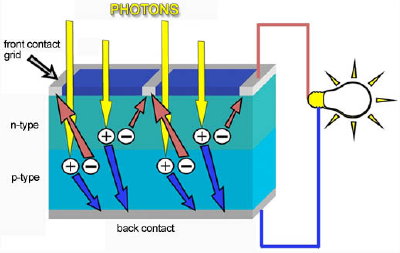
When photons hit the photovoltaic cell, freed electrons (-) attempt to unite with holes on the p-type silicon layer. The p-n junction, a one-way road, only allows the electrons to move in one direction. If we provide an external conductive path, electrons will flow through this path to their original (p-type) side to unite with holes.
The electron flow provides the current ( I ), and the photovoltaic cell's electric field causes a voltage ( V ). With both current and voltage, we have power ( P ), which is just the product of the two. Therefore, when an external load (such as an electric bulb) is connected between the front and back contacts, electricity flows in the photovoltaic cell, working for us along the way.
Sources:http://www.physics.org/article-questions.asp?id=51
Credit: http://specmat.com/photovoltaic%20cell%20specmat.html
No comments:
Post a Comment